
LNA MMIC PROJECT
Fall 2016
During the Fall 2016 semester at Tufts University I designed a two stage distributed MMIC LNA using the available gain design approach.


Single Stage Designs
The first step of the design process was to determine the lumped component matching networks for the input and output matching networks of both stages of the amplifier. These matching networks were designed using the Smith Chart tools in ADS.


Interstage Matching Network Design
The interstage matching network was designed using the ADS Smith Chart based matching network designer. The matching network was designed such that the output impedance of the first amplifier stage and the input impedance of the second amplifier stage were in agreement with their single stage output and input impedances, respectively.

Distributed Components and EM Modeling and Simulation in Momentum
After the lumped component representations of the LNA were set up, the lumped components were converted into distributed elements using the microstrip design tool in ADS. An EM simulation of the circuit was performed and the design of matching networks was iterated based on the difference between the expected results and the EM performance characteristics.


Results
After validating the initial output data, a few iterations of EM optimization led to the final performance parameters shown below.


2.0 - 2.5 GHZ LNA DESIGN IN ADS
Spring 2015
During the Spring of 2015 semester at Tufts University I designed a single stage lumped component LNA. Some of the highlights are shown below.
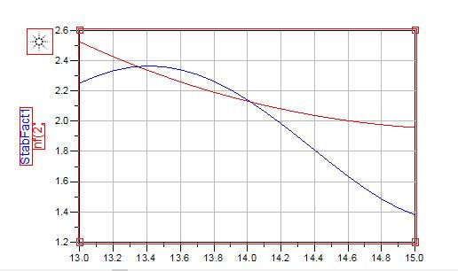
The first step of the design was bringing the stability factor of the amplifier circuit above 1 over all operating frequencies using a shunt resistor at the output. A 12.5 ohm resistor was used to bring the stability factor above 1 for the frequency range.


An inductor and a resistor were placed in series from the input to the output to generate negative feedback for a more flat gain response.


The input and output matching networks were then designed for the LNA. Each network was matched to 50 Ohms.


The EM model of the circuit is shown below along with the S-Parameter data accompanying the EM model.


INTERDIGITAL FILTER DESIGN IN MOMENTUM
Fall 2013

INTERDIGITAL FILTER DESIGN IN MOMENTUM
Fall 2017
In my first semester at Tufts I designed an interdigital filter using ADS Momentum.
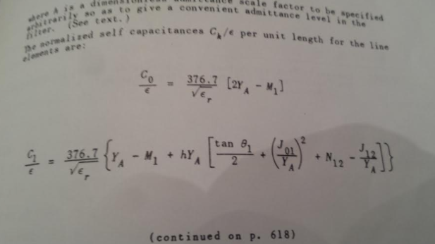
The geometry of the filter such as the bar width, length and spacing were designed based on the relations between the relative bandpass filter bandwidth and the coupling coefficients between each resonator.


The tables for coupling coefficients for the bandpass filter are shown in the table pictured to the left from Mathaei, Jones and Young.


The S-Parameters for the bandpass filter are shown below.


MICROSTRIP PATCH ANTENNA DESIGN IN HFSS
Fall 2017
In Fall 2017 at Tufts University I designed a microstrip patch antenna using the design procedure for a broadside array from Balanis. At the conclusion of the modeling and simulation in HFSS I had the antenna fabricated and measured the S-Parameters and gain.


The dimensions of the antenna were calculated based on the equations for a microstrip patch antenna width and length from Balanis. The measured directivity of the broadside antenna in HFSS was approximately 16 dB, which met design standards. The gerber files were then sent to a manufacturer to fabricate the antenna PCB.


The measured antenna gain, shown in the bottom right plot below aligned well with the simulated value for directivity in HFSS, which was roughly 16 dB.


